Formation of Moiré Interlayer Excitons in Space and Time – Publication by B9 (Malic) in Nature

A large research team including Ermin Malic and coworkers observed the formation of a “dark” moiré interlayer exciton for the first time

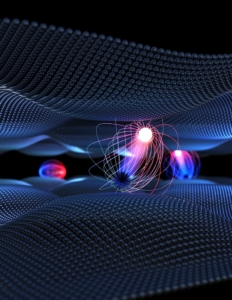
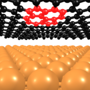
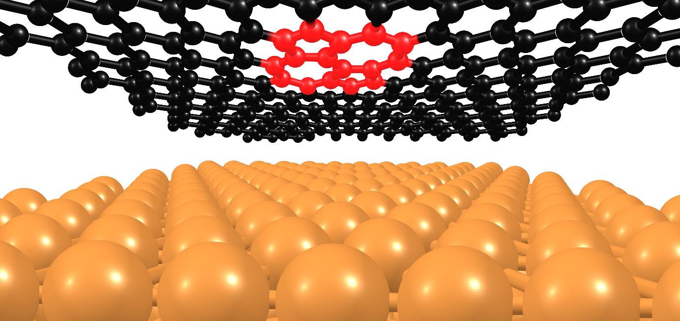
A large number of so-called optically dark excitons form between two twisted layers of tungsten diselenide (top) and molybdenum disulfide (bottom) after optical excitation. (Reprinted with permission from Nature, link see below)

Atomically thin structures made of two-dimensional semiconductor materials are promising candidates for future devices in electronics, optoelectronics and photovoltaics. The properties of these semiconductors can be controlled by stacking atomically thin layers on top of each other. However, the angle of rotation in the structure of the semiconductors can be adjusted as desired, and this angle of rotation is of interest for the production of novel solar cells. Typical experimental approaches have only indirect access to the moiré interlayer excitons and are blind to the ‘dark’ excitons.

An international research team including Ermin Malic and coworkers from the SFB succeeded in directly visualizing so-called dark moiré interlayer excitons by using time-resolved ARPES measurements combined with microscopic many-particle theory. The researchers show how the time-resolved momentum microscopy provides deepest microscopic insights into these technologically relevant questions.

These results not only provide a fundamental insight into the formation of dark moiré interlayer excitons, but also open up a new perspective to study the optoelectronic properties of these new and fascinating materials, e.g., the signature of the moiré potential and the influence of the combined properties of the two twisted semiconductor layers.

For further information, please see the press release by the university of Göttingen (in German).

Publication

D. Schmitt, J.P. Bange, W. Bennecke, A.A. Al Mutairi, G. Meneghini, K. Watanabe, T. Taniguchi, D. Steil, D.R. Luke, R.T. Weitz, S. Steil, G.S.M. Jansen, S. Brem, E. Malic, S. Hofmann, M. Reutzel, S. Mathias
Formation of moiré interlayer excitons in space and time
Nature 608 (2022) 499 DOI:10.1038/s41586-022-04977-7

Contact

Prof. Dr. Ermin Malic
Philipps-Universität Marburg
SFB 1083 project B9
Tel.: 06421 28-22640
EMAIL

Topological Stone–Wales Defects Enhance Bonding and Electronic Coupling at the Graphene/Metal Interface – Publication by A4 (Gottfried) and A6 (Tonner) in ACS Nano

Benedikt Klein and coworkers of SFB 1083, together with external collaborators, have gained new insight into interfacial interactions of Stone-Wales graphene defects by using molecular models.

Graphene is an astonishing two-dimensional material with diverse and technologically important properties. However, these properties are heavily dependent on topological defects, which have a direct impact on the graphene/metal interface. A common defect is the Stone-Wales (SW) defect, consisting of two five- and two seven-membered rings resulting in a non-alternating bonding situation.  Researchers of the SFB 1083 projects A4 (Gottfried) and A6 (Tonner) investigated the interface between a SW defect and a metal by mimicking the defect with the molecule azupyrene. Pyrene was used as a model for defect-free graphene of the same size as azupyrene. The experiments were complemented by extensive modelling of the graphene-embedded defects.

Figure: Graphene/metal interface with typical topological defect. The local interaction of a topological S–W graphene defect with a metal surface is mimicked by azupyrene, which allow the application of a wide range of experimental techniques. Copyright 2022 American Chemical Society.

In the present work, it was shown by a multi-technique approach (XPS/UPS, NIXSW, NEXAFS, TPD, LT-AFM, DFT) that the embedded defects, modelled by azupyrene, undergo enhanced bonding and electron transfer with a Cu(111) surface. This indicated by increased bond energies of 68 kJ/mol, by 0.9 Å reduced bond distances and enhanced charge transfer. The consistent experimental results were corroborated by DFT calculations.

The defect-induced enhanced electronic coupling at the graphene/metal interface is expected to have significant impact on the performance of (opto-)electronics, e.g., by increasing charge injection rates. Tailoring the topological structure of graphene layer may result in the development of new or imprived devices.

Publication

B.P. Klein, A. Ihle, S.R. Kachel, L. Ruppenthal, S.J. Hall, L. Sattler, S.M. Weber, J. Herritsch, A. Jaegermann, D. Ebeling, R.J. Maurer, G. Hilt, R. Tonner-Zech, A. Schirmeisen, J.M. Gottfried
Topological Stone–Wales Defects Enhance Bonding and Electronic Coupling at the Graphene/Metal Interface
ACS Nano (2022) DOI:10.1021/acsnano.2c01952

Contact

Prof. Dr. J. Michael Gottfried
Philipps-Universität Marburg
SFB 1083 project A4
Tel.: 06421 28-22541
EMAIL

On the Role of Collective Electrostatic Effects in Electronic Level Pinning and Work Function Changes by Molecular Adlayers: The Case of Partially Fluorinated DNTTs Adsorbed Flat-Lying on Various Metals and Hetero-Structures – Publication by A2 (Witte) and A8 (Koert)

In a new publication in Advanced Materials Interfaces, the groups of Gregor Witte (A2), Ulrich Koert (A8) as well as Jérôme Cornil from the University of Mons report on the formation of an internal interface dipole at a metal/2D metal/organic hetero-interface, which can be modified by the outer organic monolayer.

Schematic representation of the outer and internal interface dipoles at the FxDNTT/cesium/copper hetero-interface (Image: Maximilian Dreher, CC BY-NC-ND 4.0).

The use of organic contact layers is a versatile tool to control the work function of metal electrodes. While partial fluorination of robust organic molecules leads to a significant shift of their frontier energy levels in the isolated molecules, this effect can be wiped out for organic films adsorbed on high work function metal substrates leading to an equalization of the corresponding HOMO levels. Consequently, also the work function shift is equalized in the condensed phase, which is often referred to as HOMO (resp. LUMO) level pinning. Especially the LUMO level pinning has been reported only on a theoretical level in literature yet.

By using partially fluorinated DNTTs, which were synthesized by project A8 and exhibit such a HOMO level pinning on high work function noble metals, the group of Jérôme Cornil (Mons, Belgium) demonstrated that a LUMO level pinning also exists on low work function Cs(110) surfaces on a theoretical level. To face low work function surfaces experimentally, Maximilian Dreher and coworkers used atomically thin cesium layers that grow epitaxial on Cu(100) single crystals and provide more inert, low work function surfaces. In contrast to the expectation, this copper/cesium/organic hetero-stack reveals no LUMO pinning effect. Complementary DFT calculations demonstrate, that the contributions prevailing on the work function shift can be separated into (i) an outer interface dipole between the organic layer and the 2D cesium layer and (ii) an inner, buried interface dipole at the metal/cesium interface. While the outer interface dipole is again equalized for the different FxDNTT species, the buried interface dipole is modulated dependent on the degree of fluorination of the molecules.

Such a sandwich hetero-interface provides new possibilities to effectively tailor contact layers between metal electrodes and active organic layers improving their energy level alignment and emphasizes the importance of internal interfaces.

Publication

M. Dreher, D. Cornil, M. W. Tripp, U. Koert, J. Cornil, G. Witte
On the Role of Collective Electrostatic Effects in Electronic Level Pinning and Work Function Changes by Molecular Adlayers: The Case of Partially Fluorinated DNTTs Adsorbed Flat-Lying on Various Metals and Hetero-Structures
Adv. Mater. Interfaces (2022) DOI:10.1002/admi.202200361

Contact

Prof. Dr. Gregor Witte
Philipps-Universität Marburg
SFB 1083 project A2
Tel.: 06421 28-21384
EMAIL