F-Center Mediated Growth of Patterned Organic Semiconductor Films on Alkali Halides – Publication by A2 (Witte)

In a combined experimental and theoretical study, the groups of Gregor Witte (A2) and Jérôme Cornil from the University Mons present a new approach of patterning organic semiconductor films with simultaneous molecular orientation control based on an electrostatic stabilization at the film/substrate interface in the presence of F-centers in alkali halide substrates created by controlled electron irradiation.

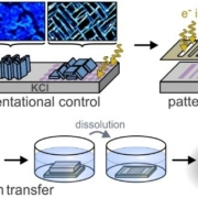
Scheme of the process chain that allows transfer of patterned organic films to any non-water-soluble substrate. Reprinted with permission from ACS Appl. Mater. Interfaces 2022. Copyright 2022 American Chemical Society.

A key problem in organic electronics remains the lateral patterning and structuring of organic films for device applications since photo­lithography is not applicable due to the lack of chemical robustness of the organic materials in the etching process. Therefore, alternative approaches are necessary for the patterning of organic films.

In this study, Darius Günder et al. demonstrate that electron irradiation of KCl(100) substrates induces surface localized F-centers (halide vacancies) that strongly influence the molecular orientation and lateral structure of subsequently grown organic films. By combining AFM, SEM and XRD measurements they show for the case of dinaphto­thieno­thiophene (DNTT) that molecules adopt a recumbent molecular orientation and form elongated fibers while hexagonally shaped islands with upright orientation are present on pristine KCl. Interestingly, both morphologies exhibit epitaxial alignments that are understood by higher-order commensurabilities. A complementary DFT-based theoretical analysis in the group of Jérôme Cornil identified electrostatic interactions between F-centers and interfacial DNTT molecules as origin of the different film morphologies. Furthermore, shadow masks or electron beam lithography techniques also allow spatially selective surface irradiation to generate patterns of F-centers, and thus enable lateral structuring of DNTT films.

Finally, it could be shown that due to the water solubility of the alkali halide growth templates, the patterned organic films can also be transferred to other substrates, including amorphous elastomeric plastic substrates, while the lateral and orientational order remain fully intact, hence underlining the great potential of this new patterning method for device applications.

Publication

D. Günder, V. Diez-Cabanes, A. Huttner, T. Breuer, V. Lemaur, J. Cornil, G. Witte
F-Center-Mediated Growth of Patterned Organic Semiconductor Films on Alkali Halides
ACS Appl. Mater. Interfaces (2022) DOI:10.1021/acsami.2c13934

Contact

Prof. Dr. Gregor Witte
Philipps-Universität Marburg
SFB 1083 project A2
Tel.: 06421 28-21384
EMAIL

Obituary for Prof. Dr. Stephan W. Koch – Nachruf für Prof. Dr. Stephan W. Koch

Die Mitglieder des Sonderforschungsbereichs 1083 „Struktur und Dynamik innerer Grenzflächen“ trauern um Prof. Dr. Stephan W. Koch, der im September 2022 im Alter von 69 Jahren verstorben ist.

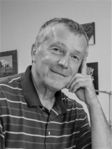
Foto: Tim van de Bovenkamp; Copyright: SFB 1083

Stephan W. Koch promovierte 1979 in Frankfurt und war von 1977 bis 1984 wissenschaftlicher Mitarbeiter am Institut für Theoretische Physik der Universität Frankfurt, an dem er auch bereits 1983 habilitierte. Nach drei Jahren als Stipendiat der F. Thyssen-Stiftung und der DFG im Rahmen eines Heisenberg-Stipendiums ging er 1986 als Associate Professor an das Physics Department and Optical Sciences Center der University of Arizona in Tucson, wo er 1989 zum Full Professor ernannt wurde. 1993 kam er dann nach Marburg und übernahm in Nachfolge von Otfried Madelung und Stefan Schmitt-Rink den Lehrstuhl für Theoretische Festkörperphysik an der Philipps-Universität Marburg, wobei er weiterhin Adjunct Professor an der University of Arizona blieb. Diesen beiden Stationen blieb er bis zu seiner Pensionierung treu.

Seine Forschungsschwerpunkte lagen auf dem Gebiet der theoretischen Festkörperphysik. Besonders interessierten ihn hier die theoretischen Grundlagen der Wechselwirkung von Licht mit Materie in Halbleitermaterialien sowie in Laserstrukturen und Mikro-Resonatoren.

Stephan W. Koch war ein herausragender, international hoch angesehener Wissenschaftler. Durch seine Arbeiten zur Vielteilchenphysik und den optoelektronischen Eigenschaften von Halbleitern trug er maßgeblich zum heutigen Verständnis von Festkörpern und insbesondere Halbleiternanostrukturen bei. Für seine Leistungen wurde er 1997 mit dem Leibniz-Preis der Deutschen Forschungsgemeinschaft (DFG) sowie 1999 mit dem Max-Planck-Forschungspreis der Alexander-von-Humboldt-Stiftung und der Max-Planck-Gesellschaft ausgezeichnet.

Stephan Koch hat die Forschungslandschaft der Marburger Physik entscheidend mitgeprägt. Von 1995 bis 2001 leitete er den erfolgreichen SFB 383 „Disorder on mesoscopic scales“ und war seit 2013 Mitglied des SFB 1083 „Structure and dynamics of internal interfaces“.

Stephan Koch verstand es, seine vielen Schülerinnen und Schüler für die Halbleiterphysik zu begeistern. Viele von Ihnen sind heute an Hochschulen und Forschungseinrichtungen tätig.

Mit großer Dankbarkeit und Anerkennung werden wir uns an ihn als einen stets aufgeschlossenen Kollegen erinnern, der in seinem gesamten Schaffen immer wieder neue Impulse gegeben und Zeichen gesetzt hat.

Unser tiefes Mitgefühl und unsere Anteilnahme gelten seiner Ehefrau und seinen Angehörigen.

Wir werden ihn vermissen.


Formation of Moiré Interlayer Excitons in Space and Time – Publication by B9 (Malic) in Nature

A large research team including Ermin Malic and coworkers observed the formation of a “dark” moiré interlayer exciton for the first time

A large number of so-called optically dark excitons form between two twisted layers of tungsten diselenide (top) and molybdenum disulfide (bottom) after optical excitation. (Reprinted with permission from Nature, link see below)

Atomically thin structures made of two-dimensional semiconductor materials are promising candidates for future devices in electronics, optoelectronics and photovoltaics. The properties of these semiconductors can be controlled by stacking atomically thin layers on top of each other. However, the angle of rotation in the structure of the semiconductors can be adjusted as desired, and this angle of rotation is of interest for the production of novel solar cells. Typical experimental approaches have only indirect access to the moiré interlayer excitons and are blind to the ‘dark’ excitons.

An international research team including Ermin Malic and coworkers from the SFB succeeded in directly visualizing so-called dark moiré interlayer excitons by using time-resolved ARPES measurements combined with microscopic many-particle theory. The researchers show how the time-resolved momentum microscopy provides deepest microscopic insights into these technologically relevant questions.

These results not only provide a fundamental insight into the formation of dark moiré interlayer excitons, but also open up a new perspective to study the optoelectronic properties of these new and fascinating materials, e.g., the signature of the moiré potential and the influence of the combined properties of the two twisted semiconductor layers.

For further information, please see the press release by the university of Göttingen (in German).

Publication

D. Schmitt, J.P. Bange, W. Bennecke, A.A. Al Mutairi, G. Meneghini, K. Watanabe, T. Taniguchi, D. Steil, D.R. Luke, R.T. Weitz, S. Steil, G.S.M. Jansen, S. Brem, E. Malic, S. Hofmann, M. Reutzel, S. Mathias
Formation of moiré interlayer excitons in space and time
Nature 608 (2022) 499 DOI:10.1038/s41586-022-04977-7

Contact

Prof. Dr. Ermin Malic
Philipps-Universität Marburg
SFB 1083 project B9
Tel.: 06421 28-22640
EMAIL