Enhanced Circular Dichroism and Polarized Emission in an Achiral, Low Band Gap Bismuth Iodide Perovskite Derivative

Johanna Heine (A15) and Sangam Chatterjee (B2) successfully prepared a novel iodido bismuthate that shows strong optical activity despite being achiral

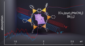
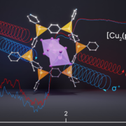
Reprinted with permission from J. Am. Chem. Soc. 2023. Copyright 2023 American Chemical Society.

Lead halide perovskites and related main group halogenido metalates offer unique semiconductor properties and diverse applications in photovoltaics, solid-state lighting, and photocatalysis. Recent advances in incorporating chiral organic cations have led to the emergence of chiral metal-halide semiconductors with intriguing properties such as chiroptical activity and chirality-induced spin selectivity. This enables the generation and detection of circularly polarized light and spin-polarized electrons for applications in spintronics and quantum information, fields that use the spin of electrons or photons to store and process data.

However, understanding the structural origin of chiroptical activity remains challenging due to macroscopic factors and experimental limitations. In general, chiroptical activity originates in the crystal symmetry of the solid state. However, the compound does not need to be chiral to exhibit chiroptical activity. Some non-centrosymmetric crystal classes are sufficient as well – a fact that is often overlooked in current research.

The groups of Dr. Heine (A15) and Prof. Chatterjee (B2) present a novel achiral perovskite derivative [Cu2(pyz)3(MeCN)2][Bi3I11] (pyz = pyrazine; MeCN = acetonitrile), that exhibits remarkable circular dichroism. Notably, single crystals display linear and circular optical activity as well as a significant degree of circularly polarized photoluminescence. The magnitude of these effects on par or even larger than what can be achieved by incorporating chiral organic molecules into perovskites. These findings provide insights into the macroscopic origin of circular dichroism and offer design guidelines for developing materials with high chiroptical activity without expensive chiral building blocks.

Publication

J. Möbs, P. Klement, G. Stuhrmann, L. Gümbel, M. Müller, S. Chatterjee, J. Heine
Enhanced Circular Dichroism and Polarized Emission in an Achiral, Low Band Gap Bismuth Iodide Perovskite Derivative
J. Am. Chem. Soc. 145 (2023) 23478 DOI:10.1021/jacs.3c06141

Contact

Dr. Johanna Heine
Philipps-Universität Marburg
SFB 1083 project A15
Tel.: 06421 28-25482
EMAIL

34. Erfinderlabor: Scientific curiosity of the next Generation

Hessen’s young MINT scientists conduct research on hydrogen and renewable energies within the SFB 1083 and Philipps University Marburg

Group foto of the closing event.

The 34th Inventors’ Lab (Erfinderlabor) of the Center for Chemistry (Zentrum für Chemie, ZFC) has successfully entered its finale. This year’s event was once again organized by the ZFC in cooperation with the Philipps University of Marburg and Elkamet and supported by other renowned cooperation partners such as the SFB 1083.

The practice-oriented workshop not only offers valuable career orientation on career opportunities in the MINT environment (mathematics, informatics, natural sciences and technology), but also always addresses a current topic of high socio-political and economic relevance. The focus of this years Inventors’ Lab was on renewable energies and hydrogen.

The sixteen students in four teams dealt with different issues in the context of the energy transition in different research groups, which are part of the SFB 1083. The topics were novel crystalline materials for the use of surface structures as energy converters, the functioning of batteries and the basics of laser spectroscopy as well as the self-construction of a spectrometer. Finally, the storage of hydrogen in metal hydrides was investigated.

The experts were impressed by the technical curiosity and quick comprehension, but also by the motivation and team spirit of the young people. “Here, a highly complex topic was explained precisely,” said Prof. Dr. Gregor Witte from the SFB during the virtual closing event.

The local project partner was the Chemikum Marburg represented by Dr. Christof Wegscheid-Gerlach. “The Inventors’ Lab exemplifies how scientific topics of the future can be communicated at the intersection of school and university, and thus how both levels of education can be interlinked.”

Contact

Dr. Christof Wegscheid-Gerlach
Philipps-Universität Marburg
SFB 1083 project Oe
Tel.: 06421 28-25843
EMAIL

Measuring spatially-resolved potential drops at semiconductor hetero-interfaces using 4D-STEM– Publication by A5 (Volz) in Small Methods

The team of project A5 of the SFB successfully measured the potential drop across a hetero interface using four-dimensional scanning transmission electron microscopy

Copyright by Wiley, 2023.

Characterizing long-range electric fields and built-in potentials in functional materials at nano to micrometer scales is of supreme importance for optimizing devices. For example, the functionality of semiconductor heterostructures or battery materials is determined by the electric fields established at interfaces, which can also vary spatially. In this study, we propose momentum-resolved four-dimensional scanning transmission electron microscopy (4D-STEM) for the quantification of these potentials. So far, dynamic effects have inhibited the quantitative evaluation of fields at heterointerfaces. The scientists in SFB project A5 carefully adopted their experimental setup to overcome these challenges and for the first time quantitatively measured the potential drop across a GaAs/AlAs interface.

In detail, a precession electron diffraction (PED) system was introduced, which rocks the impinging electron beam at a rate of 1 kHz, while scanning across the sample. This significantly reduces the impact of dynamic effects in the 4D data. In turn, an energy filter minimizes the influence of inelastic scattering.

Using the method proposed, allows the quantification of intentional or parasitic electric fields even in the presence of heterointerfaces. Accordingly, the characterization of real-life devices, like solar cells or battery materials, which often involve a multitude of such internal interfaces, becomes feasibly to optimize their performance.

Publication

V. Chejarla, S. Ahmed, J. Belz, J. Scheunert, A. Beyer, K. Volz
Measuring spatially-resolved potential drops at semiconductor hetero-interfaces using 4D-STEM
Small Methods (2023) 2300453 DOI:10.1002/smtd.202300453

Contact

Prof. Dr. Kerstin Volz
Philipps-Universität Marburg
SFB 1083 project A5, A14, B13
Tel.: 06421 28-22297
EMAIL