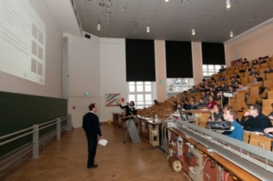
Kick-Off Meeting of the SFB 1083

Official start of the Collaborative Research Centre 1083 “Structure and Dynamics of Internal Interfaces”

November 27th – 29th, 2013
Philipps-Universität Marburg – Department of Physics – Renthof 5, GrHs

More information on the SFB 1083 Kickoff meeting_online.

New Publication by A2 (Witte)

Structure of Molecular Acceptor-Donor Interfaces: The Case of Pentacene and C60

Organic photovoltaic (OPV) cells based on conjugated polymers or small molecular weight organic compounds have attracted substantial research attention in the last decade due to their potential to provide clean and low-cost electrical energy. Unfortunately, the complex interface structure of polymer blends has so far largely hampered microscopic studies on the energetics and dissociation dynamics of photo-generated excitons formed at the involved donor-acceptor junctions. Aiming to improve the understanding of the microstructure and energetics of molecular hetero-structures, prototypical model interfaces between small molecular weight organic
compounds that form crystalline films, such as Buckminster fullerene (C60) and pentacene (PEN), are of particular interest. Although mutual conformations and the exact structure of the interface between both compounds are theoretically proposed to have significant impact on the actual device characteristics, the microstructure of
these interfaces had so far hardly been addressed in previous works.

In a current study of the working group Molecular Solids (Prof. G. Witte) which was just published in the journal ACS Applied Materials & Interfaces, the interface between the organic semiconductors pentacene and fullerene has been investigated by combining microscopy (AFM, SEM) with diffraction (XRD) and x-ray absorption spectroscopy (NEXAFS) techniques. It was demonstrated that utilizing the anisotropic interaction between different molecular compounds and tuning the effective diffusion length enables structural control over nanostructures. To understand the interface formation in detail, well-defined, crystalline pentacene multilayers have been used as support, on which small amounts of C60 have been deposited. By adjusting the substrate temperature during growth, the effective diffusion length was tuned and a site specific nucleation was achieved which allows or suppresses C60 nucleation at step edges, or even activates diffusion along step edges yielding separated
but edge-pinned C60 clusters. As a result, C60-adlayer structures of different dimensionality have been realized ranging from planar films (2D) to step decorated chains (1D) to clusters (0D). Interestingly, all these different structures are found to be fully stable at room temperature. It was further demonstrated that such 1D and 0D C60 structures can be overgrown by subsequent pentacene deposition, forming a crystalline cover layer of the same orientation as the bottom layer, hence enabling the formation of low dimensional buried organic heterostructures.

The present results are an important milestone towards an understanding and controlled fabrication of interfaces between organic semiconductors and will be the basis for further spectroscopic studies of the buried C60 nanostructures that are explored in the collaborative research centre 1083 “Structure and Dynamics of Internal
Interfaces”.

Publication: T. Breuer and G. Witte
Diffusion-Controlled Growth of Molecular Heterostructures: Fabrication of Two-, One-, and Zero-Dimensional C60 Nanostructures on Pentacene Substrates
ACS Applied Materials and Interfaces (in print, 2013), DOI: 10.1021/am402868s

Press Release: Research at Interfaces

In a new collaborative research centre, physicists and chemists from Marburg are investigating the “structure and dynamics of internal interfaces”.

In a new collaborative research centre, physicists and chemists from Marburg are investigating the “structure and dynamics of internal interfaces”. This is the title of a “Sonderforschungsbereich” (SFB), whose installation has just been decided by the “Deutsche Forschungsgemeinschaft” (DFG). The physicist Professor Dr. Ulrich Höfer from the Philipps-Universität is the initiator and spokesman of the consortium, which will be supported by the DFG with 8.7 million Euros during the following four years. (Picture: Pressestelle der Philipps-Universität/Markus Farnung)

This is the title of a “Sonderforschungsbereich” (SFB), whose installation has just been decided by the “Deutsche Forschungsgemeinschaft” (DFG). The physicist Professor Dr. Ulrich Höfer from the Philipps-Universität is the initiator and spokesman of the consortium, which will be supported by the DFG with 8.7 million Euros during the following four years.

“With this funding decision the work of our researchers over many years receives its well-deserved acknowledgement”, says Professor Dr. Katharina Krause, president of the Philipps-Universität. “The university administration is extremely pleased, that the investments into materials sciences and semiconductor physics pay off in this way and we thank the involved scientists for their outstanding commitment.”

Interfaces are contact areas between different materials. They play a decisive role in miniaturized semiconductors, which are used, for example in electronic circuits. These semiconductors are constructed of several layers of different elements, similar to a sandwich cake. “The interfaces between the different materials frequently determine which optical and electronic characteristics such semiconductor devices possess”, explains Höfer.

The importance of internal interfaces will continue to increase further, when future hybrid materials combine the characteristics of metals, traditional inorganic semiconductors and organic materials”, predicts Höfer. Examples of such hybrid materials are novel solar cells and biosensors. “Our microscopic understanding of the structure and dynamics of internal interfaces, however, is lagging far behind their enormous importance.” The main cause of this knowledge gap is the experimental difficulty to detect the weak signals of the interface, which is often buried under many layers of other materials.

The initiators of the new CRC aim to close this gap by the collaboration between different research areas such as semiconductor physics, surface science, chemical synthesis, structural analysis and laser spectroscopy. For these efforts the University of Marburg offers a perfect environment because, according to the DFG referees, the combined expertise in these research areas is worldwide unique at this location. The list of the participating scientists includes 15 groups of the Faculties of Physics and Chemistry, of the Materials Sciences Center, and of a guest project of the Basque institution “Donostia International Physics Center”, in San Sebastián, Spain.

Initially, the investigations will not be directed towards specific functional materials as those generally consist of many, frequently not well defined interfaces. Instead, the focus will be on model systems with specially prepared internal interfaces. These interfaces will be structurally characterized on the atomic level and their optical and electronic properties will be systematically investigated.

In this way, a detailed microscopic understanding and prediction of chemical bonding, electronic coupling and energy transfer for different classes of heterointerfaces shall be achieved. “In the medium and long term this knowledge shall be used in order to tailor interfaces for new applications and construct devices with novel properties and functions”, explains Höfer.