Heteroepitaxy in Organic/TMD Hybrids and Challenge to Achieve it for TMD Monolayers: The Case of Pentacene on WS2 and WSe2 – Publication by A2 and B5

In their study published in ACS Applied Materials & Interfaces, Darius Günder, Marleen Axt and Gregor Witte reveal an epitaxial alignment of organic films on crystalline TMD substrates and demonstrate strategies for achieving this intrinsic van der Waals epitaxy, which is very sensitive to surface defects of the underlying 2D material, also for exfoliated monolayers.

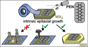
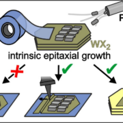
Comparison of different approaches to achieve the intrinsic epitaxy of PEN films on exfoliated and transferred TMD monolayers (Image: D. Günder, Reprinted with permission from ACS Appl. Mater. Interfaces 2024. Copyright 2024 American Chemical Society.)

The intriguing photophysical properties of monolayer stacks of different transition-metal dichalcogenides (TMDs) have recently prompted an extension of similar investigations on the interfacial excitonic coupling to hybrid systems of TMDs and organic films, as the latter combine large photoabsorption cross-section with the ability to tailor energy levels by targeted synthesis. In order to achieve such an excitonic coupling in momentum space a defined azimuthal alignment of the molecular adsorbate is crucial, which occurs on highly defined 2D material surfaces. However, this intrinsic van der Waals epitaxy of crystalline organic films cannot be automatically transferred to every 2D material surface because surface defects caused by exfoliation and transfer can result in significantly different film structures without any epitaxial order. 

In this combined study of projects A2 and B5, Darius Günder et al. used X-ray diffraction, optical polarization, and atomic force microscopy to resolve the epitaxial alignment of crystalline pentacene (PEN) films grown at the basal plane of WS2 and WSe2 samples. While (022)-oriented PEN films with recumbent molecular orientation are formed on both studied TMDs, the azimuthal orientation of the long molecular axis is quite different. Moreover, it is shown that this intrinsic epitaxial growth of PEN films depends sensitively on the TMD surface quality. While it occurs on exfoliated TMD single crystals and multilayer flakes, it is hardly found on exfoliated and transferred monolayers, which often exhibit bubbles and wrinkles. This enhances the surface roughness and results in (001)-oriented PEN films with upright molecular orientation but without any azimuthal alignment. However, monolayer flakes can be smoothed by AFM operated in contact mode or by transferring TMD monolayers to ultrasmooth substrates such as hBN, which again yields epitaxial PEN films, but with significantly smaller domains than on TMD single crystals.

The presently demonstrated existence of epitaxial crystalline organic adlayers on TMDs paves the way for future investigations of interface or moiré excitons in such hybrid systems and also highlights the challenges in fabricating organic/TMD hybrid systems with well-defined interfaces.

Publication

D. Günder, M. Axt, G. Witte
Heteroepitaxy in Organic/TMD Hybrids and Challenge to Achieve it for TMD Monolayers: The Case of Pentacene on WS2 and WSe2
ACS Appl. Mater. Interfaces (2023) DOI:doi.org/10.1021/acsami.3c15829

Contact

Prof. Dr. Gregor Witte
Philipps-Universität Marburg
SFB 1083 project A2
Tel.: 06421 28-21384
EMAIL

Layer-by-layer deposition of organic molecules controlled by selective click reactions – Publication by A8 (Koert/Dürr) in Chemistry of Materials  

In a joint effort, the research groups led by Ulrich Koert and Michael Dürr realized the controlled layer-by-layer synthesis of organic molecular structures on silicon.

Two selective click reactions are employed for the controlled layer-by-layer synthesis or organic structures on silicon. Each reaction step is performed in solution and monitored by means of X-ray photoelectron spectroscopy under ultra-high vacuum conditions. Reprinted with permission from Chem. Mater. 2024. Copyright 2024 American Chemical Society.

The application of molecular layer deposition on silicon surfaces may open the route to directly synthesizing organic molecular architectures with tailored physical and/or physicochemical properties on the technologically most relevant silicon substrates (“more than Moore”). 

In their most recent publication, the researchers from A8 show how to use a combination of two selective and orthogonal click reactions (Cu-mediated and strain promoted azide-alkyne couplings) for such a controlled layer-by-layer growth of organic architectures on Si(001). Starting point was the Si(001) substrate, which was selectively functionalized with a substituted cyclooctyne under ultrahigh-vacuum (UHV) conditions. The subsequent layer-by-layer synthesis using the two orthogonal click chemistry reaction steps was then performed in solution in an alternating fashion. The product of each reaction step was analyzed in UHV by means of X-ray photoelectron spectroscopy; controlled layer-by-layer growth up to 11 molecular layers was realized and monitored in this way.

Together with previous studies of the researchers from A8 (Koert/Dürr), B5 (Höfer/Mette) and A6 (Tonner) on selective functionalization of the Si(001) surface and the combination of UHV-based surface chemistry with solution-based click chemistry, a complete toolbox for the well-controlled growth of molecular structures on silicon is now available.

Publication

T. Glaser, J.A. Peters, D. Scharf, U. Koert, M. Dürr
Layer-by-Layer Deposition of Organic Molecules Controlled by Selective Click Reactions
Chem. Mater. 36 (2024) 561 DOI:10.1021/acs.chemmater.3c02707

Contact

Prof. Dr. Ulrich Koert
Philipps-Universität Marburg
SFB 1083 project A8
Tel.: 06421 28-26970
EMAIL

Prof. Dr. Michael Dürr
Justus-Liebig-Universität Gießen
SFB 1083 project A8
Tel.: 0641 99-33490
EMAIL

Enhanced Circular Dichroism and Polarized Emission in an Achiral, Low Band Gap Bismuth Iodide Perovskite Derivative

Johanna Heine (A15) and Sangam Chatterjee (B2) successfully prepared a novel iodido bismuthate that shows strong optical activity despite being achiral

Reprinted with permission from J. Am. Chem. Soc. 2023. Copyright 2023 American Chemical Society.

Lead halide perovskites and related main group halogenido metalates offer unique semiconductor properties and diverse applications in photovoltaics, solid-state lighting, and photocatalysis. Recent advances in incorporating chiral organic cations have led to the emergence of chiral metal-halide semiconductors with intriguing properties such as chiroptical activity and chirality-induced spin selectivity. This enables the generation and detection of circularly polarized light and spin-polarized electrons for applications in spintronics and quantum information, fields that use the spin of electrons or photons to store and process data.

However, understanding the structural origin of chiroptical activity remains challenging due to macroscopic factors and experimental limitations. In general, chiroptical activity originates in the crystal symmetry of the solid state. However, the compound does not need to be chiral to exhibit chiroptical activity. Some non-centrosymmetric crystal classes are sufficient as well – a fact that is often overlooked in current research.

The groups of Dr. Heine (A15) and Prof. Chatterjee (B2) present a novel achiral perovskite derivative [Cu2(pyz)3(MeCN)2][Bi3I11] (pyz = pyrazine; MeCN = acetonitrile), that exhibits remarkable circular dichroism. Notably, single crystals display linear and circular optical activity as well as a significant degree of circularly polarized photoluminescence. The magnitude of these effects on par or even larger than what can be achieved by incorporating chiral organic molecules into perovskites. These findings provide insights into the macroscopic origin of circular dichroism and offer design guidelines for developing materials with high chiroptical activity without expensive chiral building blocks.

Publication

J. Möbs, P. Klement, G. Stuhrmann, L. Gümbel, M. Müller, S. Chatterjee, J. Heine
Enhanced Circular Dichroism and Polarized Emission in an Achiral, Low Band Gap Bismuth Iodide Perovskite Derivative
J. Am. Chem. Soc. 145 (2023) 23478 DOI:10.1021/jacs.3c06141

Contact

Dr. Johanna Heine
Philipps-Universität Marburg
SFB 1083 project A15
Tel.: 06421 28-25482
EMAIL