Growth of extended DNTT fibers on metal substrates by suppression of step-induced nucleation – Publication by A2 (Witte)
In their study published in Nanoscale Horizons, Maximilan Dreher, Dayeon Kang, Tobias Breuer and Gregor Witte introduce and validate a new concept to suppress the defect-driven fiber nucleation at surface steps by selective blocking of the active step sites using small molecules, so that the formation of crystalline, organic fibers is only governed by the intrinsic epitaxial growth on ideal, defect-free surface regions.
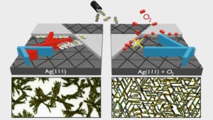
DNTT fiber structures grown on Ag(111) substrates without (left) and with (right) pre-exposition of oxygen to the surface. The oxygen suppresses the DNTT molecules to adsorb at the step edges, which leads to straight, elongated and epitaxially aligned fibers. (Image: M. Dreher). Reproduced with permission from the Royal Society of Chemistry.
Due to their anisotropic optoelectronic properties, crystalline organic fibers constitute an interesting class of nanoscale materials with great potential for integration into future optoelectronic devices based on organic-inorganic hybrid systems. While chemical synthesis allows for flexible tailoring of electronic molecular properties, well-established structuring methods such as, e.g. lithography are hardly applicable to most molecular materials. Therefore, self-organization is an important alternative route for structuring molecular materials especially for organic/inorganic hybrid architectures. While molecular materials often form crystalline fibers, their length and orientation is, however, limited by surface defects such as steps of the supports that cannot be prevented even on very perfect, single crystalline substrates, hence drastically restricting their use in device applications.
In their study the authors analyzed the influence of surface step edges on the initial growth of fibers for the case of the high performing organic semi¬conductor dinaphthothienothiophene (DNTT) and developed a new concept to suppress the defect–driven fiber nucleation. Based on a comparison of the organic film growth on densely packed, flat noble metal surfaces and on a regularly stepped, vicinal surface, they first showed how substrate steps affect the azimuthal molecular orientation in the seed layer and also the subsequent fiber formation. In a next step they demonstrate that this parasitical step-induced fiber nucleation that occurs also on densely packed Ag(111) surfaces can be suppressed by first exposing the metal support to oxygen, or even briefly to ambient condition, which causes a selective saturation of the active step sites. They show that this not only leads to an exclusive growth of epitaxial DNTT fibers but also strongly increases the fiber size to several hundreds of microns. This novel approach is quite versatile and allows a distinct improvement of template assisted growth and thereby the quality of organic/inorganic hybrids.
Publication
M. Dreher, D. Kang, T. Breuer and G. Witte,
Growth of extended DNTT fibers on metal substrates by suppression of step-induced nucleation
Nanoscale Horizons (2019) DOI:10.1039/C9NH00422J
Poster Award
The paper’s first author Maximilian Dreher is currently a Master’s student within SFB-project A2. We congratulate him on receiving the prize for his poster on the above research which he presented at the Cecam Workshop on “Fabrication processes and molecular organization in organic thin films: Theory and simulation meet experiments” held in Lecco, Italy from July 17-20, 2019.
Contact
Prof. Dr. Gregor Witte
Philipps-Universität Marburg
SFB 1083 project A2
Tel.: 06421 28 21384
EMAIL
 Semiconductor surfaces are the basis for microtechnology and major applications like photovoltaics. Improving their efficiency and applicability toward future demands on materials requires functionalization with suitable molecules. Fundamental research can help here to understand the interaction between molecules and surfaces.
 In his thesis entitled “Charge carried dynamics and photocurrents in the Dirac cone of topological insulators” Johannes Reimann investigated a novel class of materials, topological insulators. These materials, discovered only a decade ago, are insulating in the volume, but conductive at their surfaces and at their interfaces with conventional materials.