Synthesis of 2D Gallium Sulfide with Ultraviolet Emission by MOCVD – Publication by A4 (Gottfried), A5 (Volz), A14 (Volz) and B2 (Chatterjee) in Small

In a joint study of the projects A4, A5, A14 and B2, the two-dimensional growth of GaS on sapphire by MOCVD was successfully studied and the layers were characterized using a wide variety of techniques.

2D materials exhibit the potential to transform semiconductor technology. Their rich compositional and stacking varieties allow tailoring materials’ properties toward device applications. Monolayer to multilayer GaS, with its ultraviolet band gap, which can be tuned by varying the layer number, holds promise for solar‐blind photodiodes and light‐emitting diodes as applications.

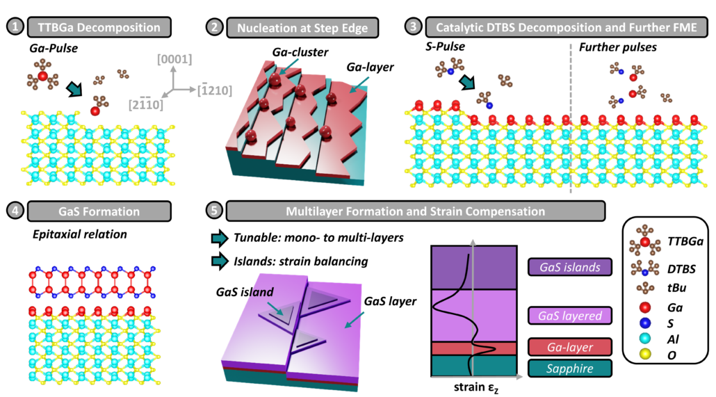
In this cooperative study of different groups within the SFB 1083, the one‐step synthesis of 2D GaS is introduced via MOCVD (metal–organic chemical vapor deposition) on sapphire substrates. The pulsed‐mode deposition of industry‐standard precursors promotes 2D growth by inhibiting the vapor phase and on‐surface pre‐reactions. High resolution STEM imaging proves the ML nature of the GaS, but also shows a covalently bonded Ga adlayer on the sapphire, which plays an important role in mediating the epitaxial relationship of the GaS ML with respect to the sapphire substrate. The structural and chemical composition determined by electron microscopy related techniques are corroborated by XRR, XPS, Raman spectroscopy and PL and confirm a 2D nucleation of GaS on sapphire, which is an intricate balance between surface wetting, Ga droplet formation and strain-induced change of atomic spacing as well as van der Waals distances.

Growth model of the flow modulated GaS deposition.

The results highlight the adaptability of established growth facilities for producing atomically thin to multilayered 2D semiconductor materials, paving the way for practical applications.

Publication

O. Maßmeyer, R. Günkel, J. Glowatzki, P. Klement, B. Ojaghi Dogahe, S.R. Kachel, F. Gruber, M. Müller, M. Fey, J. Schörmann, J. Belz, A. Beyer, J.M. Gottfried, S. Chatterjee, K. Volz
Synthesis of 2D Gallium Sulfide with Ultraviolet Emission by MOCVD
Small (2024) 2402155 DOI:10.1002/smll.202402155

Contact

Prof. Dr. Kerstin Volz
Philipps-Universität Marburg
SFB 1083 project A5, A14, B13
Tel.: 06421 28-22297
EMAIL

Probing electron-hole Coulomb correlations in the exciton landscape of a twisted semiconductor heterostructure – Publication by B9 (Malic) in Science Advances

In a joint study including the experimental group of Stefan Mathias from the University of Göttingen and the theoretical group of Ermin Malic the ultrafast charge transfer in twisted van der Waals heterostructures was studied.

Cover of Science Advances Volume 10 Issue 6. An ultrashort light pulse breaks apart an exciton, comprised of an electron bound to an electron hole.

In two-dimensional semiconductors, cooperative and correlated interactions determine the material’s excitonic properties and can even lead to the creation of correlated states of matter.

In a joint experiment theory study, the research groups of Stefan Mathias (Göttingen) and Ermin Malic (Marburg) have studied the ultrafast charge transfer in twisted van der Waals heterostructures.  The researchers found that the transfer of an excitons hole across a type II band-aligned heterostructure leads to an unexpected sub-200-femtosecond upshift of the single-particle energy of the electron being photoemitted from the two-particle exciton state. While energy relaxation usually leads to an energetic downshift of the spectroscopic signature, is was shown that this upshift is a clear fingerprint of the correlated interaction of the electron and hole parts of the exciton.

In this way, time-resolved photoelectron spectroscopy is straightforwardly established as a powerful method to access electron-hole correlations and cooperative behavior in quantum materials. The joint work highlights this capability and motivates the future study of optically inaccessible correlated excitonic and electronic states of matter.

Publication

J.P. Bange, D. Schmitt, W. Bennecke, G. Meneghini, A.A. Al Mutairi, K. Watanabe, T. Taniguchi, D. Steil, S. Steil, R.T. Weitz, G.S.M. Jansen, S. Hofmann, S. Brem, E. Malic, M. Reutzel, S. Mathias
Probing electron-hole Coulomb correlations in the exciton landscape of a twisted semiconductor heterostructure
Sci. Adv. 10 (2024) eadi1323 DOI:10.1126/sciadv.adi1323

Contact

Prof. Dr. Ermin Malic
Philipps-Universität Marburg
SFB 1083 project B9
Tel.: 06421 28-22640
EMAIL

Heteroepitaxy in Organic/TMD Hybrids and Challenge to Achieve it for TMD Monolayers: The Case of Pentacene on WS2 and WSe2 – Publication by A2 and B5

In their study published in ACS Applied Materials & Interfaces, Darius Günder, Marleen Axt and Gregor Witte reveal an epitaxial alignment of organic films on crystalline TMD substrates and demonstrate strategies for achieving this intrinsic van der Waals epitaxy, which is very sensitive to surface defects of the underlying 2D material, also for exfoliated monolayers.

Comparison of different approaches to achieve the intrinsic epitaxy of PEN films on exfoliated and transferred TMD monolayers (Image: D. Günder, Reprinted with permission from ACS Appl. Mater. Interfaces 2024. Copyright 2024 American Chemical Society.)

The intriguing photophysical properties of monolayer stacks of different transition-metal dichalcogenides (TMDs) have recently prompted an extension of similar investigations on the interfacial excitonic coupling to hybrid systems of TMDs and organic films, as the latter combine large photoabsorption cross-section with the ability to tailor energy levels by targeted synthesis. In order to achieve such an excitonic coupling in momentum space a defined azimuthal alignment of the molecular adsorbate is crucial, which occurs on highly defined 2D material surfaces. However, this intrinsic van der Waals epitaxy of crystalline organic films cannot be automatically transferred to every 2D material surface because surface defects caused by exfoliation and transfer can result in significantly different film structures without any epitaxial order. 

In this combined study of projects A2 and B5, Darius Günder et al. used X-ray diffraction, optical polarization, and atomic force microscopy to resolve the epitaxial alignment of crystalline pentacene (PEN) films grown at the basal plane of WS2 and WSe2 samples. While (022)-oriented PEN films with recumbent molecular orientation are formed on both studied TMDs, the azimuthal orientation of the long molecular axis is quite different. Moreover, it is shown that this intrinsic epitaxial growth of PEN films depends sensitively on the TMD surface quality. While it occurs on exfoliated TMD single crystals and multilayer flakes, it is hardly found on exfoliated and transferred monolayers, which often exhibit bubbles and wrinkles. This enhances the surface roughness and results in (001)-oriented PEN films with upright molecular orientation but without any azimuthal alignment. However, monolayer flakes can be smoothed by AFM operated in contact mode or by transferring TMD monolayers to ultrasmooth substrates such as hBN, which again yields epitaxial PEN films, but with significantly smaller domains than on TMD single crystals.

The presently demonstrated existence of epitaxial crystalline organic adlayers on TMDs paves the way for future investigations of interface or moiré excitons in such hybrid systems and also highlights the challenges in fabricating organic/TMD hybrid systems with well-defined interfaces.

Publication

D. Günder, M. Axt, G. Witte
Heteroepitaxy in Organic/TMD Hybrids and Challenge to Achieve it for TMD Monolayers: The Case of Pentacene on WS2 and WSe2
ACS Appl. Mater. Interfaces (2023) DOI:doi.org/10.1021/acsami.3c15829

Contact

Prof. Dr. Gregor Witte
Philipps-Universität Marburg
SFB 1083 project A2
Tel.: 06421 28-21384
EMAIL