Turning at top speed – Publication by B11 (Güdde/Höfer) in Nature
In collaboration with the group of Rupert Huber in Regensburg, Suguru Ito, Jens Güdde and Ulrich Höfer from the new SFB project B11 “Ultrafast dynamics of interface currents” demonstrate efficient high-order harmonic generation at the surface of a topological insulator by driving ballistic electron currents at THz frequencies.

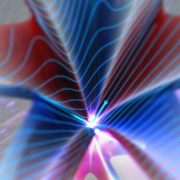
On the surface of a topological insulator (colored surface), electrons (small blue sphere) move with quasi-relativistic speed. When a strong light wave accelerates electrons through the so-called Dirac point (apex of the cone), their velocity abruptly flips. The instantaneous change of velocity leads to the emission of broadband electromagnetic radiation (flash in the middle of the colored surface). Reprinted with permission from Nature (link see below).
In the conducting surface states of topological insulators electrons behave like massless particles, characterized by a linear dispersion (Dirac cone). Under the influence of an electric field, the electrons rapidly switch their direction of motion when their trajectories in momentum come close to the minimum of the cone, the Dirac point. At frequencies in the range of 25 to 35 THz, this is the case for electric field strengths of several MV/cm. It results in the emission of an ultrafast flash of light containing a broadband spectrum up to frequencies of 800 THz that can be analyzed with optical detectors.
This novel mechanism of high-harmonic generation is only possible because the spin-momentum-locking in the Dirac cone prevents efficient electron scattering. The resulting long scattering times of ~1 ps allow to drive strong ballistic electron currents as demonstrated previously with THz-ARPES (Reimann et al. Nature 2018). The emitted high-harmonic radiation has a characteristic polarization dependence related to the Berry curvature of the Dirac cone. Moreover, it can be shifted to arbitrary non-integer multiples of the driving frequency by varying the carrier-envelope phase of the driving field. These specific properties set it apart from HHG processes in bulk semiconductors (Hohenleutner et al. Nature 2015).
In the upcoming third funding period, SFB 1083 will utilize THz high-harmonic radiation generated in this way and exploit its characteristic properties to investigate electron currents at interfaces of topological insulators buried under protecting capping layers. For future device applications, it will be crucial to screen the unusual movement of Dirac electrons from the environment.
Informational Material
– Press release of the university of Regensburg (in English and German).
– Press release of the university of Marburg (in German).
– News of Physics Department, Philipps-Universität Marburg (in German).
– Homepage of the Huber group in Regensburg.
Publication
C.P. Schmid, L. Weigl, P. Grössing, V. Junk, C. Gorini, S. Schlauderer, S. Ito, M. Meierhofer, N. Hofmann, D. Afanasiev, J. Crewse, K.A. Kokh, O.E. Tereshchenko, J. Güdde, F. Evers, J. Wilhelm, K. Richter, U. Höfer, R. Huber
Tuneable non-integer high-harmonic generation in a topological insulator
Nature (2021) DOI:10.1038/s41586-021-03466-7
Contact
Prof. Dr. Ulrich Höfer
Philipps-Universität Marburg
SFB 1083 project B6, B11
Tel.: 06421 28 24215
EMAIL