Quantitative imaging of electric surface potentials with single-atom sensitivity
C. Wagner, M. F. B. Green, M. Maiworm, P. Leinen, T. Esat, N. Ferri, N.Friedrich, R. Findeisen, A. Tkatchenko, R. Temirov, F. S. Tautz
Nature Materials 18 (2019) 853
Coulomb interaction’s long range allows large-scale structures and their electric signals to outshine smaller ones. This makes isolation and quantification of electric potentials originating from nanoscale objects (atoms or molecules) very challenging. A newly developed non-contact scanning probe technique employs a quantum dot sensor and joint electrostatic screening by tip and surface, thus enabling quantitative surface potential imaging across all relevant length scales down to single atoms.
Electrostatic interaction is key to the functionality of many nanoscale materials and systems including the performance of organic and inorganic semiconductor devices which are affected by electric dipoles at the relevant interfaces. As the few-nanometer scale becomes evermore relevant in device concepts, the ability to measure microscopic electric potentials in functional materials and devices becomes an increasing necessity. It is these electric potentials that can provide valuable insight into primary mechanisms at surfaces and interfaces, such as reconstruction or relaxation, mechanical distortion, charge transfer and chemical interaction, which all create electric potentials at the atomic scale.

Principle of electric potential sensing with a molecular quantum dot.
State of the art in electric potential imaging at surfaces is Kelvin probe force microscopy (KPFM), but at the level of single atoms or molecules and novel semiconductor devices, KPFM is problematic as high resolution imaging can only be reached at small tip–surface distances, i.e., where chemical forces start acting and interfering with a quantitative interpretation of the data.
A novel technique called scanning quantum dot microscopy (SQDM) may solve this problem. In this approach a single molecule is attached to the tip of a non-contact atomic force/scanning tunnelling microscope (NC-AFM/STM) by controlled manipulation.The molecule may then act as a quantum dot (QD) and can be used as a sensor to detect and image electric potentials. Rigorous analysis of the corresponding imaging mechanism, by making use of the formalism of electrostatic boundary value problems, shows that SQDM can indeed be used to quantitatively map out surface potential distributions and dielectric surface topographies.
In addition, the observed effect of the screening action of the combined tip/surface system inducing an exponential decay of electric potentials with lateral distance from the probing tip allows for an exceptionally high lateral resolution of the SQDM. Detailed nvestigation of this exponential screening forms the basis of an image deconvolution algorithm that, together with far-reaching instrumental developments, transforms SQDM into a powerful imaging technique for electric surface potential imaging in ever smaller nanostructures and novel materials.

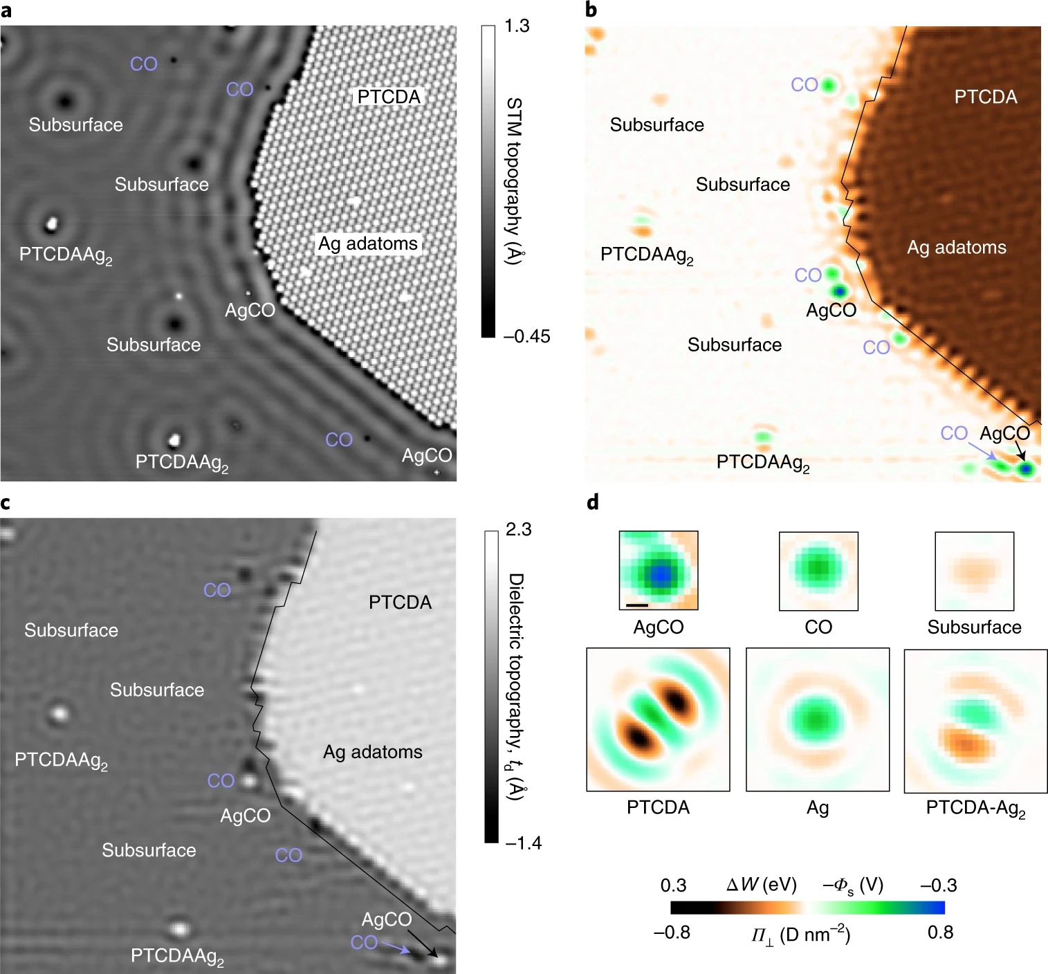
SQDM images of nanostructures on Ag(111). (a) STM image (60 × 60 nm2) showing various adsorbates and defects on a Ag(111) surface. (b) SQDM surface potential image. (c) SQDM dielectric topography image. (d) SQDM images of individual nanostructures including a PTCDA–Ag2 complex. Scale bar, 1 nm.


