
Smaller, faster, more efficient? – Review by A5 (Volz)
In their review paper, Andreas Beyer and Kerstin Volz describe in detail their investigation of novel composite materials, which may eventually replace today’s silicon-based electronic devices. As the latter increasingly reach their performance limit, one option to overcome these largely physics-based limitations is to cover silicon with a different material layer.
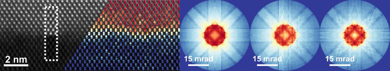
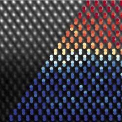
Experimentally measured and simulated structure of the galliumphospide/silicon-interface at atomic resolution. Electron diffraction patterns allow to determine the interfacial charge distribution.
However, covering silicon with different material layers like, for example, well-suited III/V semiconductors (containing elements of the 3rd and 5th group of the periodic system) is challenging. In joining different materials with their individual physico-chemical properties their interface may be marked by defects. Here, for example, “erroneous” attachments may lead to unwished-for local charges – rendering the combined material as unsuitable for application in devices.
The group of Kerstin Volz closely studied galliumphosphide on silicon as a model system of III/V semiconductors on silicon. In their invited review the authors now describe the various electron-microscopy-based approaches employed in the study of the internal interface between the two materials and its defects. By means of transmission-electron-microscopy the researchers were able to show that the interface between the two materials is far from smooth; in fact, it more resembles a pyramidal structure affecting several atomic layers. In addition, it was also possible to “see” the erroneous atomic attachments which cause the unwished-for charge effect and link the phenomenon directly to changes in preparatory procedures.
The insights gained will be applied to perfecting preparation methods in order to reduce the number of defects and to fine-tuning the interface with a focus on raising the efficiency of existing devices and encouraging the development of novel applications.
Publication
A. Beyer and K. Volz,
Quantitative Electron Microscopy for III/V on Silicon Integration
Adv. Mater. Interfaces (2019) DOI: 10.1002/admi.201801951
Contact
Prof. Dr. Kerstin Volz
Philipps-Universität Marburg
SFB 1083 project A5
Tel.: 06421 28 22297
EMAIL